
Overview / Summary
BITS Pilani's Center for Research Excellence in Semiconductor Technologies (CREST) serves as a center for state-of-the-art semiconductor research, innovation, and cooperation. With its cutting-edge facilities, wide range of focus areas, and solid industry relationships, CREST is well-positioned to contribute significantly to the development of India's semiconductor capabilities and the education of the country's future workforce.
More details about CREST-> https://crest.bits-pilani.ac.in/
Vision
To make BITS Pilani as the leading academic institution for Semiconductor Research and Innovation in India
Mission
To be at the forefront of India’s Mission Level Programs (Semiconductors, Cyber Physical Systems, and Quantum Tech)
Aim & Objectives
- Industry Ready Professionals with career placements in the Semiconductor sector
- Cutting-edge innovations, Intellectual Property, and Research Publication
- An established ecosystem (infrastructure, resources, and know-how) for students, researchers, and startups
Campus
Pilani Campus
Dubai Campus
Goa Campus
Hyderabad Campus
Focus areas or Specializations of Center
CREST concentrates on several important areas:
Materials: Studying photonics, composites, and 2D materials for cutting-edge semiconductor applications.
Devices: Creation of photonic integrated circuits, FETs, MEMS, and microfluidics.
Applications include advancements in energy harvesting, cyber-physical systems, smart sensors, and environmental technologies.
IoT, quantum, and AI/ML technologies are being investigated in semiconductor research.
Key facilities or Resources provided by the Center
Modern facilities are available at CREST to facilitate cutting-edge research:-
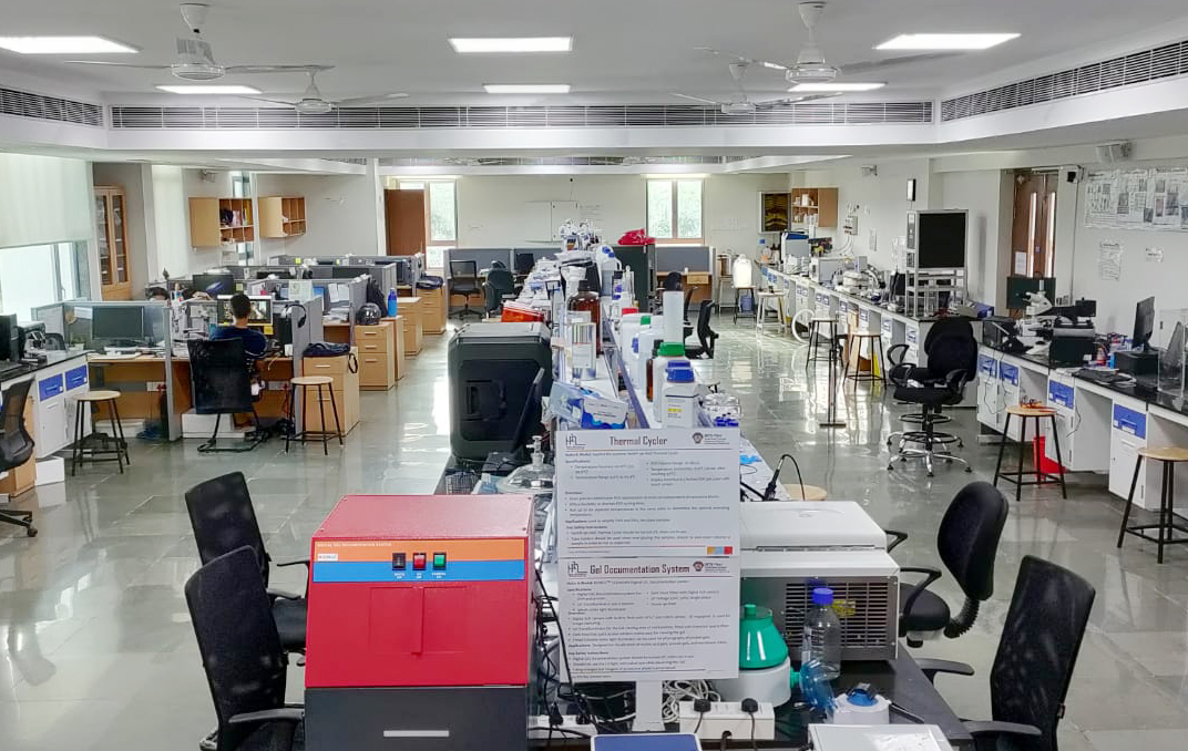
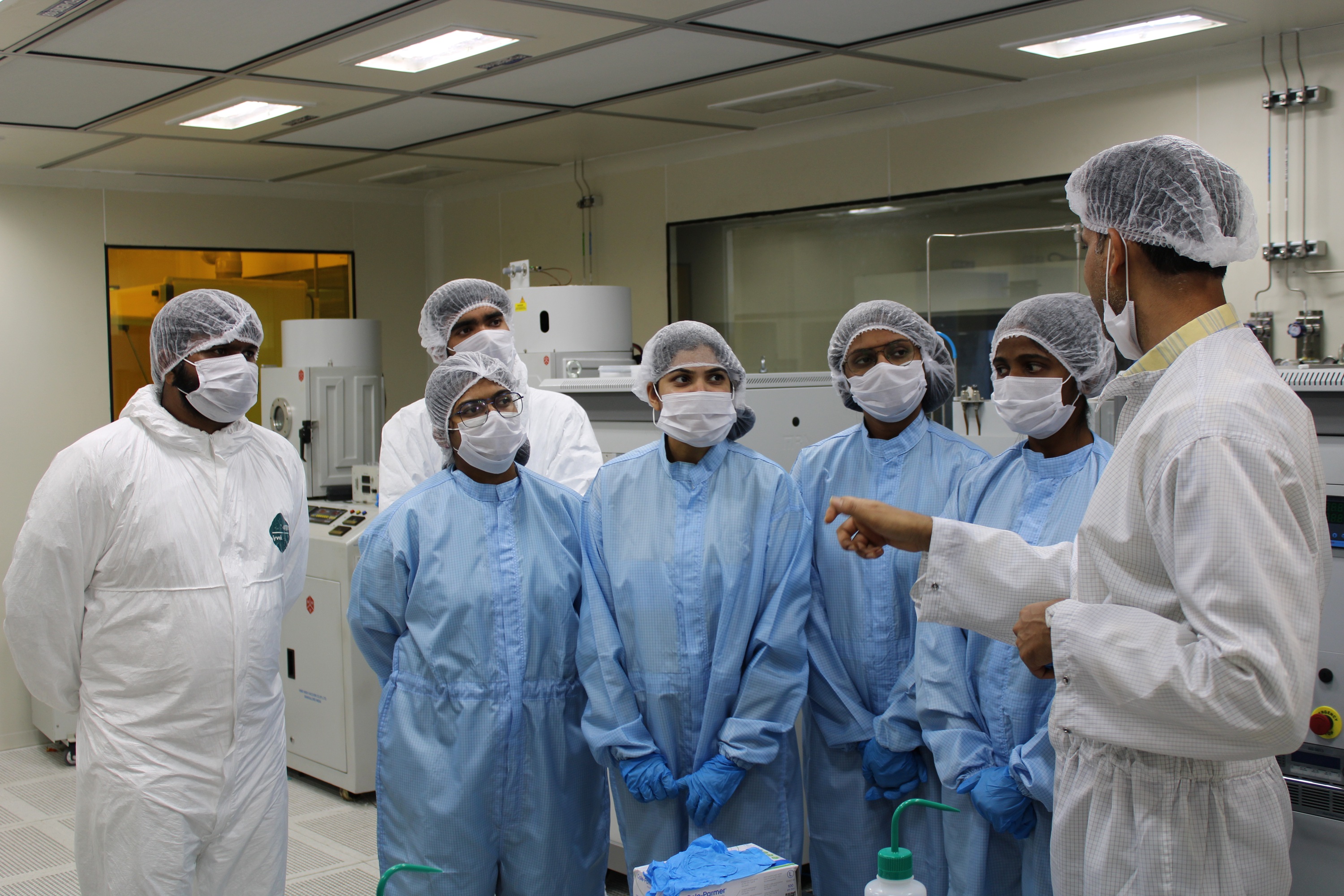
Facilities for Cleanrooms: Class 100 and Class 1000 cleanrooms furnished with equipment such as spin coaters, mask aligners, RF sputter deposition systems, reactive ion etching systems, diffusion furnaces, and wet chemical benches.
Nuclear Magnetic Resonance (NMR) Spectroscopy, High-Performance Thin Layer Chromatography (HPTLC), X-Ray Diffraction (XRD) systems, Atomic Force Microscope (AFM), Confocal Laser Scanning Microscope, Raman Spectrometer, and Field Emission Scanning Electron Microscope (FESEM) are among the instruments in the Central Analytical Laboratory.
Future Additions: Tools to improve fabrication and testing capabilities, such as the Micro Universal Testing Machine (UTM), Wire Bonder, Pulse Measurement Unit, and E-Beam Lithography
Services
- CREST offers a range of services to encourage innovation and research:
- Research Support: Helping to carry out cutting-edge semiconductor technology research initiatives.
- Industry Collaboration: Joint research and development partnerships with government organizations, startups, and multinational semiconductor corporations.
- Startup Incubation: Assistance for new businesses via the MeitY Startup Hub and partnerships with institutions like as T-Hub Telangana.
- Consultancy Services: Professional guidance and solutions for industrial partners involved in the development of semiconductors.
Training & Workshops
Professional Development Courses: Online courses such as "Introduction to Device and System Packaging" are designed for postgraduate students, academic professors, and industry engineers and are created in partnership with international experts.
Workshops: Activities centered on semiconductor technology, sensors, AI/ML applications, and sustainable development, such as ICAN 1.0 and the Indo-Norway Workshop.
Monthly Colloquia: Ongoing conferences with leading academics and business executives talking about developments in semiconductors, artificial intelligence, sensors, and materials engineering.
Student Internship Programs: Practical instruction for students from different universities to encourage women in STEM and give them a taste of semiconductor manufacturing and research